FEMTO Engineering is an R&D center of the foundation FC Innov
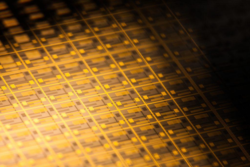
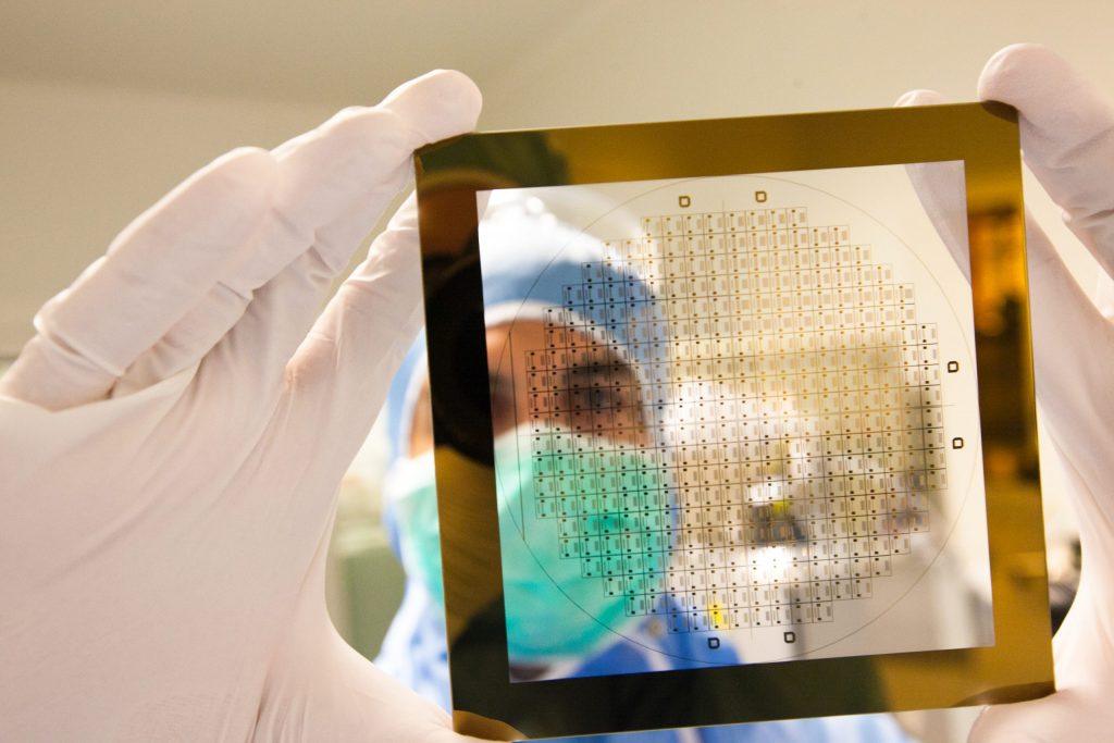
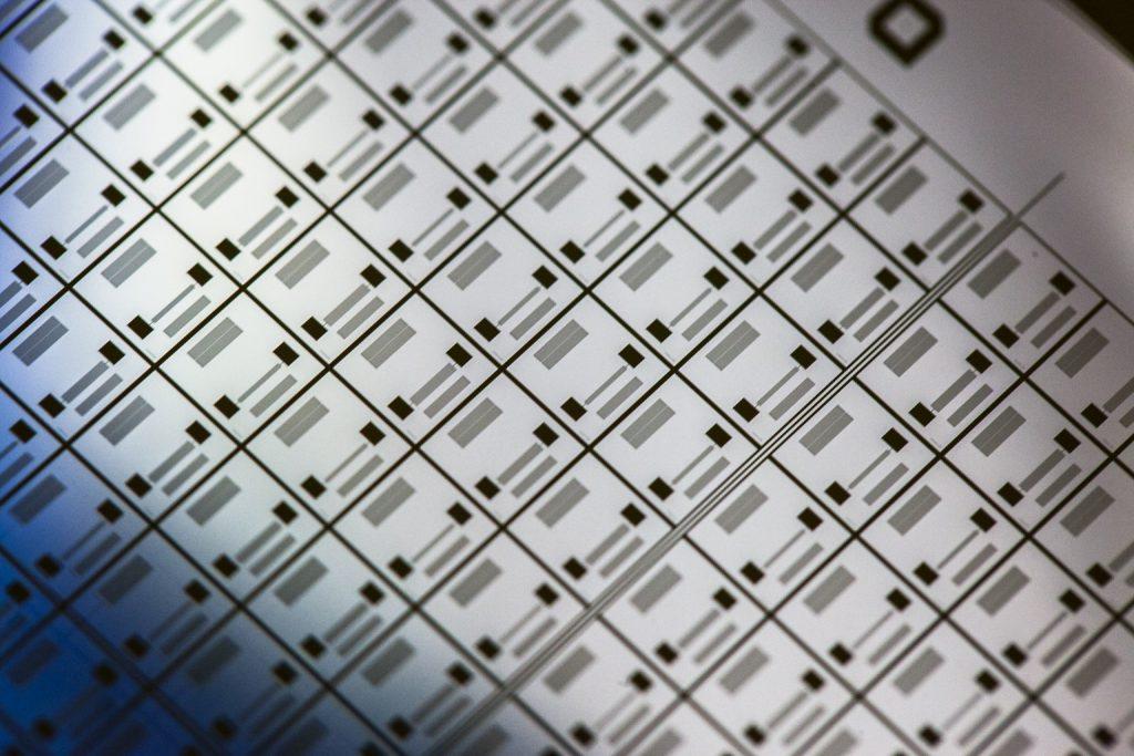
Microfabrication in a clean room allows the realization of structures and components on the micrometric and nanometric scales, with a mastery of processes and materials inaccessible outside a controlled environment. It is the core technology of MEMS, microsystems, precision optical components and many biomedical devices.
FEMTO Engineering offers manufacturers an access to the processes and equipment of the MIMENTO clean room at the FEMTO-ST institute. MIMENTO is certified ISO 5 to 7 and ISO 9001, and is part of the national RENATECH network. The team supports projects from process definition to component delivery, ensuring the interface between industrial needs and the platform’s technological capacities.
You need structures at the micrometric and nanometric scale, on specific materials, with tolerances that conventional machining cannot reach. You do not have access to a clean room or the necessary microfabrication processes.
You have an idea for a component or device but you do not know if the process is feasible with your materials, nor which parameters to use. You need an exploration and testing phase before committing.
You validated a concept and you need to move to limited production for qualification, testing or marketing phases, without investing in your own clean room equipment.
You work on difficult substrates—quartz, sapphire, LiNbO3, diamond—which require specific processes that are not available with conventional subcontractors.
Your project requires an ISO controlled environment to ensure the cleanliness and fabrication repeatability, but investing in your own clean room is not justified for your production volume.
Assessment of material/process compatibility, initial cleanroom tests, results report.
Development of custom processes on Si, glasses, quartz, sapphire, diamond, LN, LT. Optimization, documentation, and transfer.
Access to FEMTO Engineering equipment and expertise for occasional or recurring needs.
Production in limited quantities for qualification, validation and market launch.
Precision cutting and polishing, wire bonding, wafer bonding, flip-chip microassembly.
Microsensors, microactuators, resonators, gyroscopes, accelerometers. For manufacturers who develop embedded systems or measuring instruments requiring miniaturized and reliable components.
Diffraction gratings, waveguides, ridge structures on LN, PPLN and PPLT components for nonlinear optics. For optical system manufacturers who need components on special substrates with off-catalogue specifications.
Biochips, lab-on-chips, microreactors for biological analysis, filtration membranes, microfluidic structures in biocompatible materials. For teams developing medical devices or biological analysis tools requiring controlled environment manufacturing.
Micro-gears, springs, precision parts in Si3N4 and other hard materials. For watch and fine mechanics manufacturers who need components with tight geometric tolerances and guaranteed mechanical properties.
Substrates for integrated circuits, packaging of precision electronic components, components for RF applications. For teams working on high frequency electronic systems requiring controlled deposition and etching processes.
FEMTO Engineering offers manufacturers a concrete access to one of the best French microfabrication platforms, without having to invest in cleanroom equipment or hire specialists.
For a project requiring micrometric or nanoscale manufacturing processes, it is a direct shortcut to world-class research capabilities, with technical support based on the industrial need and adapted to time and budget constraints.
UV and LIGA lithography for the definition of micrometric-scale patterns. Standard and thick resins (KMPR 1050).
RIE, DRIE on dielectric materials (glass, Si3N4, LN), FIB, KOH and BHF etching. Verticality of the flanks greater than 88°, roughness less than 5 nm.
Fabrication of 100% monocrystalline thin films from 1 to 300 μm of silicon, quartz, LN, LT, glass, sapphire on different types of substrates. Proprietary process ensuring the maintenance of physico-chemical properties.
SEM, AFM, ellipsometry, reflectometry, profilometry, resistivity measurements by tester under HF and BF tips.
Maximum aspect ratio of 400, flank roughness less than 5 nm, manufacture on substrates up to 4 inches.






FEMTO Engineering supports the companies in the development of advanced technologies by relying on the scientific excellence of the FEMTO-ST institute. FEMTO Engineering has a dedicated team of engineers and specialized experts at the service of your innovation projects, who are immersed among the FEMTO-ST research teams.
Our role: to transform the academic research results into concrete industrial solutions.