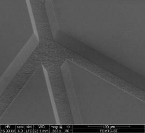
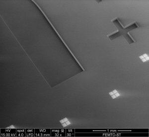
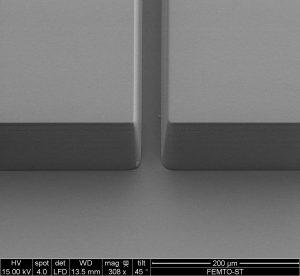
Besides silicon engraving, we have developed different methods of deep engraving of dielectric materials in clean room:
Engraved materials
Depth
Flanks verticality
Rugosité en fond de gravure
Glass
Up to 200 µm
70° at 100 µm
Ra < 500nm
Quartz
Up to 200 µm
85° at 100 µm
Ra < 10nm
Lithium niobate
Up to 10 µm
75° at 10 µm
Ra < 10nm
Benefits :
– Collective engraving of micrometric resolution patterns with depths up to a hundred microns – New features for your devices – Performance improvement of your devices
Different applications are covered:
– Structuring of microfluidic channels in biocompatible materials (Glass...) – Production of optical waveguides in electro-optical materials (Lithium Niobate...) – Etching of piezoelectric materials for radio frequency devices (Quartz…)