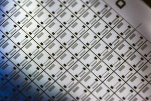
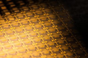
- UV & electronic lithography
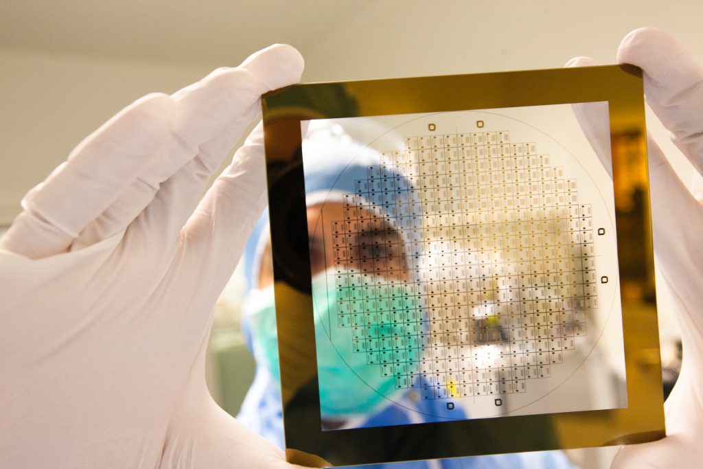
- Photolithography mask manufacturing
Deposition
Deposition of thin and thick layers

Deposition of thin and thick layers
Dry etching (ion plasma): RIE, DRIE FIB (Focus Ion Beam) Materials: Silicon (max 6 inches), Glass, Si3N4, LiNbO3,… (max 4
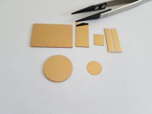
Precision cutting Lapping & polishing Wire bonding Wafer bonding Micro-assembly (flip-chip)

Microscope (MEB, optic, FIB), mechanical profilometer Specific measures : material constraints, optical index, contact angle