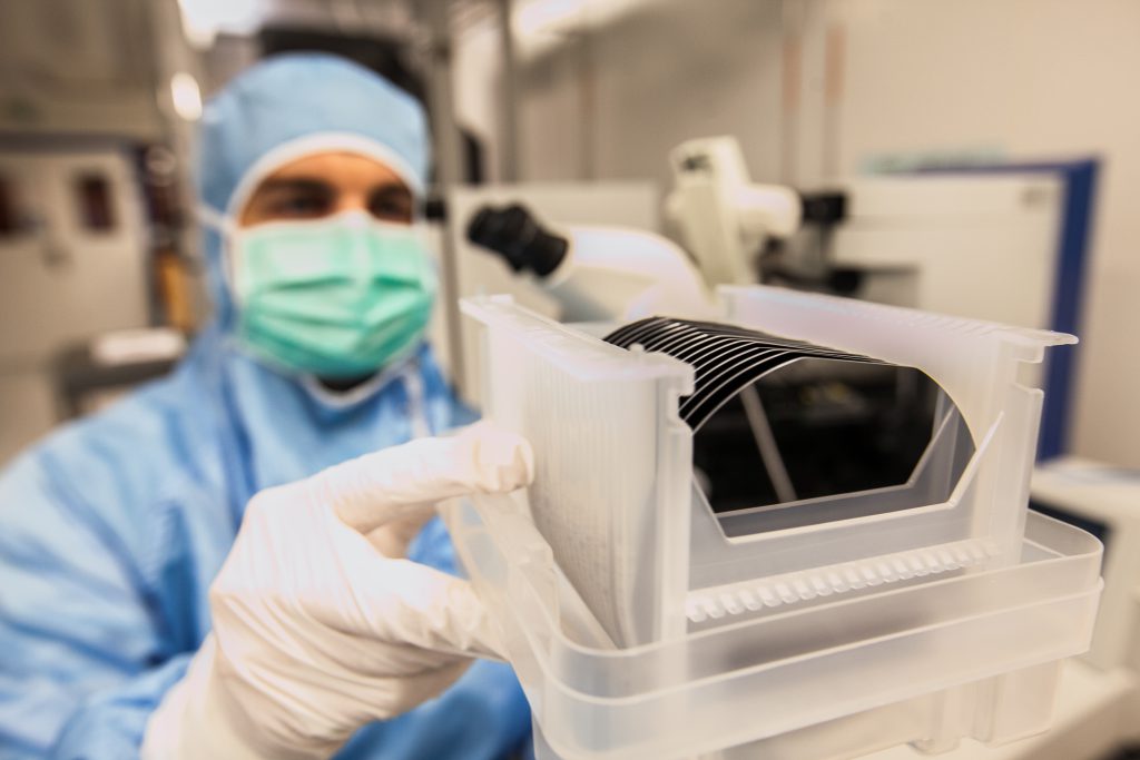
FEMTO Engineering has developed a technology to obtain custom thin monocrystalline layers transferred onto wafers with diameters up to 4 inches.

Thin monocrystalline films on electrode or insulator

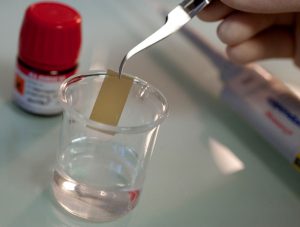
Support materials and custom thin layers among piezoelectric materials (quartz, PZT, LiNbO3),
optics (Glass, KBT, BSO …), semiconductors (Silicon) and other materials on request.

– Manufacturing of chips with plasmonic properties (SPR)
– Specific coatings (SiO2, TiO2, etc)
– Biofonctionnalization